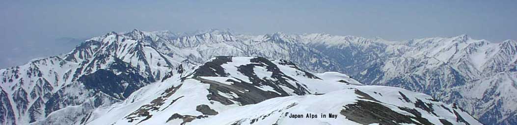
Japanese / English
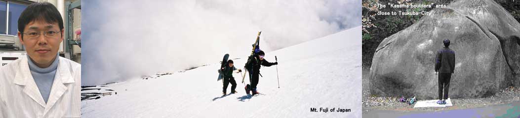
Takahide Umeda
Birth: 1971 in
Ph.D: 1999 in
Associate Professor (2003-)
Graduate
Phone&fax: +81-29-859-1307
E-mail: u m e d a @ s l i s. t s u k u b a. a c. j p
Address: 1-2 Kasuga, Tsukuba, 305-8550,
*Do not use the above addresses and numbers for
commercial use.
●We are looking for graduate students and
postdoctoral researchers●
●Graduate school,
●JSPS postdoctoral fellowships: http://www.jsps.go.jp/english/e-fellow/fellow.html
(application in every August-September and March-April)
Research
themes
Defects in semiconductors and semiconductor
devices
EDMR (electrically detected magnetic resonance)
spectroscopy
EPR (electron paramagnetic resonance) /
photo-EPR spectroscopy
Silicon (MOSFETs and LSIs)
Silicon Carbide
Diamond
Dielectric materials
Web-based databases accessible via the Internet
Scientific instruments accessible via the
Internet
Two open WEB databases for semiconductor
technologies, developed by our group
“EPR in Semiconductors”, a set of Database and Simulator for EPR centers in
Semiconductors
“Defect
Dat@base”, Knowledge Database for Defects in
Semiconductors
List of publications
[34] T. Umeda, N.T. Son, J. Isoya, N. Morishita, T. Ohshima, H. Itoh, E. Janzén
“Electron paramagnetic resonance of the HEI4/SI5 center in 4H-SiC”
Materials Science Forum 527-529, 543-546 (2006).
[33] N.T. Son, T. Umeda, J. Isoya, A. Gali, M. Bockstedte, B. Magunsson, A. Ellison, N. Morishita, T. Ohshima, H. Itoh, E. Janzén
“Divacancy model for P6/P7 centers in 4H- and 6H-SiC”
Materials Science Forum 527-529, 527-530 (2006).
[32] A. Gali, M. Bockstdete, N.T. Son, T. Umeda,
J. Isoya, E. Janzén
“Divacancy and its identification : Theory”
Materials Science Forum 527-529, 523-526 (2006).
[31] M. Bockstedte, A. Gali, T. Umeda, N.T. Son,
J. Isoya, E. Jazén
“Signature of the negative carbon vacancy-antisite complex”
Materials Science Forum 527-529, 539-542 (2006).
[30] J. Isoya, M. Katagiri, T. Umeda, N.T. Son, A. Henry, E. Janzen, T. Ohshima, N. Morishita, H. Itoh
“Shallow phosphorous donors in 3C-, 4H-, and 6H-SiC”
Materials Science Forum 527-529, 593-596 (2006).
[29] T. Umeda, K. Okonogi, K. Ohyu, S. Tsukada, K. Hamada,
S. Fujieda, Y. Mochizuki
“Single silicon vacancy-oxygen complex defect and variable retention time phenomenon in dynamic random access memories”
Applied Physics Letters 88, 253504 (2006)
[28] T. Umeda, N. T. Son, J. Isoya, E. Janzén, T. Ohshima, N. Morishita, H. Itoh, A. Gali, M. Bockstdete
“Identification of the carbon antisite-vacancy pair in 4H-SiC”
Physical Review Letters 96, 145501 (2006).
[27] N. T. Son, P. Carlsson, J. ul Hassan, E. Janzén, T. Umeda, J. Isoya, A. Gali, M. Bockstedte, N. Morishita, T. Ohshima, H. Itoh
“Divacancy in 4H-SiC”
Physical Review Letters 96,
055501 (2006)
[26] J. Isoya, M. Katagiri, T. Umeda, S. Koizumi, H. Kanda, N.T. Son, A. Henry, A. Gali, E. Janzén
“Pulsed EPR studies of Phosphorus shallow donors in diamond and SiC”
Physica B 376-377, 358-361
(2006).
[25] N.T. Son, T. Umeda, J. Isoya, A. Gali, M. Bockstedte, B. Magnusson, A. Ellison, N. Morishita, T. Ohshima, H. Itoh, E. Janzén
“Identification of divacancies in 4H-SiC”
Physica B 376-377, 334-337
(2006).
[24] T. Umeda, S. Hagiwara, M. Katagiri, N. Mizuochi, J. Isoya
“A web-based database system for EPR centers in Semiconductors”
Physica B 376-377, 249-252 (2006).
[23] N. T. Son, A. Henry, J. Isoya, M. Katagiri, T.
Umeda, A. Gali, E. Janzén
“Eelectron paramagnetic resonance and theoretical studies of shallow phosphorous centers in 3C-, 4H- and 6H-SiC”
Physical Review B 73, 075201
(2006)
[22] N. Mizuochi, S. Yamasaki, H. Takizawa, N. Morishita, T. Ohshima, H. Itoh, T. Umeda, J. Isoya
“Spin multiplicity and charge state of a silicon vacancy (Tv2a) in 4H-SiC determined by pulsed ENDOR”
Physical Review B 72, 235208
(2005)
[21] T. Umeda, Y. Ishitsuka, J. Isoya, N. T. Son, E. Janzén, N. Morishita, T. Ohshima, H. Itoh, A. Gali
“EPR and theoretical studies of negatively charged carbon vacancy in 4H-SiC”
Physical Review B 71, 193202 (2005)
[20] T. Umeda, J. Isoya, N. Morishita, T. Ohshima, T. Kamiya, A. Gali, P. Déak, N. T. Son, E. Janzén
“EPR and theoretical studies of positively charged carbon vacancy in 4H-SiC”
Physical Review B 70, 235212 (2004)
[19] T. Umeda, J. Isoya, N. Morishita, T. Ohshima, T. Kamiya
“EPR identification of two types of carbon vacancies in 4H-SiC”
Physical
Review B 69, 121201(R) (2004)
[18] T. Umeda, Y. Ishitsuka, J. Isoya,
“EPR and pulsed ENDOR study of EI6 and related defects in 4H-SiC”
Materials
Science Forum 457-460, 465-468 (2004).
[17] T. Umeda, A. Toda, Y. Mochizuki
“Measurement of process-induced defects in Si sub-micron devices by combination of EDMR and TEM”
The
European Physical Journal - Applied Physics 27, 13-20 (2004)
[16] T. Umeda, Y. Mochizuki,
K. Okonogi, K. Hamada
“Electrically detected magnetic resonance of ion-implantation damage centers in silicon large-scale integrated circuits”
Journal
of Applied Physics 94, 7106-7111 (2003)
[15] W. Futako, T. Umeda, M. Nishizawa, T. Yasuda, J. Isoya, S. Yamasaki
“In situ ESR observation of interface dangling bond formation processes during amorphous SiO2 growth on Si”
Journal of
Non-crystalline Solids 299-302, 575 (2002)
[14] T. Umeda, Y.
Mochizuki, K. Okonogi, K. Hamada
“Defects related to DRAM leakage current studied by electrically detected magnetic resonance”
Physica
B 308-310, 1169-1172 (2001)
[13] T. Umeda, M. Nishizawa, T. Yasuda, J. Isoya, S. Yamasaki, K. Tanaka
“Electron spin resonance observation of the Si(111)-(7´7) surface and its oxidation process”
Physical
Review Letters 86, 1054-1057 (2001)
[12] T. Umeda, Y. Mochizuki, Y. Miyoshi, Y. Nashimoto
“Charge-trapping defects in cat-CVD silicon nitride films”
Thin Solid Films 395, 266-269 (2001)
[11] T. Umeda, J.
Isoya, S. Yamasaki, K. Tanaka
“Microscopic origin of light-induced ESR centers in undoped hydrogenated amorphous silicon”
Physical
Review B 62, 15702-15710 (2000)
[10] T. Umeda, S. Yamasaki, M. Nishizawa, T. Yasuda, J. Isoya, K. Tanaka
“In situ electron spin resonance of initial oxidation processes of Si surfaces”
Applied
Surface Science 162-163, 299-303 (2000)
[9] T. Umeda,
“Electron spin resonance center of Dangling bonds in undoped a-Si:H”
Physical
Review B 59, 4849-4857 (1999)
[8] J.-H. Zhou, K. Ikuda, T. Yasuda, T. Umeda, S. Yamasaki, K. Tanaka
“Control of crystallinity of microcrystalline silicon film grown on insulating glass substrates”
Journal of
Non-crystalline Solids 227-230, 857-860 (1998)
[7] T. Umeda, S.
Yamasaki, A. Matsuda, J. Isoya, K. Tanaka
“Energy location of light-induced ESR centers in undoped a-Si:H”
Journal of Non-crystalline Solids 227-230, 353-357 (1998)
[6] S. Yamasaki, T. Umeda, J. Isoya, J.H. Zhou, K. Tanaka
“Microscopic nature of localized states in a-Si:H and their role in metastability”
Journal of Non-crystalline Solids 227-230, 332-337 (1998)
[5] S. Yamasaki, T.
Umeda, J. Isoya, K. Tanaka
“Existence of surface region with high dangling bond density during a-Si:H film growth”
Journal of Non-crystalline Solids 227-230, 83-87 (1998)
[4] S. Yamasaki, T.
Umeda, J. Isoya, K. Tanaka
“Insitu electron-spin- resonance measurements of film growth of hydrogenated amorphous silicon”
Applied
Physics Letters 70, 1137-1139 (1997)
[3] T. Umeda, S. Yamasaki, A. Matsuda, J. Isoya, K. Tanaka
“Electronic structure of band-tail electrons in a-Si:H”
Physical
Review Letters 77, 4600-4603 (1996)
[2] S. Yamasaki, J.-K. Lee, T. Umeda, J. Isoya, K. Tanaka
“Spatial distribution of phosphorus atoms surrounding spin centers of P-doped hydrogenated amorphous silicon elucidated by pulsed ESR”
Journal of
Non-crystalline Solids 198-200, 330-333 (1996)
[1] M. Fujita, T. Umeda,
M. Yoshida
“Polymorphism of carbon forms: Polyhedral morphology and electronic structures”
Physical
Review B 51, 13778-13780 (1995)